

Seok-min Kim
Chung-Ang University, Republic of Korea
Title: Fabrication of single crystal silicon nanowires by metal assisted chemical etching with Nano imprinted barrier pattern
Biography
Biography: Seok-min Kim
Abstract
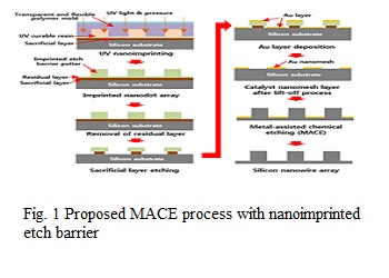
To fabricate the silicon nanowires, various methods such as vapor-liquid-solid growth, reactive ion etching with barrier pattern, oblique angle deposition and metal assisted chemical etching (MACE) have been developed. The MACE can provides a high aspect ratio and undamaged single crystal silicon nanostructures using low-cost wet etching process. In the MACE process, a patterned noble metallic structure etches the silicon substrate anisotropically in aqueous solutions containing hydrogen fluoride and an oxidant, and an isolated single crystal vertical silicon nanowires are obtained. Since the geometrical structure of silicon nanowire is mainly determined by the initial metallic pattern, the fabrication of metallic nanostructure on a silicon substrate is the key technology in the MACE process. To obtain highly ordered nanowires with precisely controlled diameter and distribution, the various metal patterning method such as electron beam lithography, photolithography and nanosphere lithography were suggested. In this study, we fabricated a highly ordered large area ultraviolet (UV) nanoimprinted etch barrier pattern on an Au catalyst layer with low cost for MACE process. A silicon nanodot master having 500nm pith, 250nm diameter and 125nm height was prepared by KrF laser scanning lithography. A transparent flexible mold was UV replicated from the silicon master, and a nanodot barrier pattern was UV imprinted on a PMMA lift-off layer coated silicon wafer. After RIE process with O2 gas, the silicon surface was exposed except nanodot barrier patterned area. An Au layer was deposited on silicon wafer using thermal evaporator and UV imprinted nanodot barrier were lift-offed with PMMA layer in acetone solution with ultrasonication process. Finally, Au nanohole array was fabricated and MACEed in hydro fluoride and hydrogen peroxide mixed aqueous solution. Depending on the etching time, 300 – 8000 nm heights silicon nanowire arrays were successfully demonstrated.
This study was supported by a grant of the Korean Health Technology R&D Project, Ministry of Health & Welfare, Republic of Korea. (HI14C2687), and the Technology Transfer Development Program (S2334634) funded by the Small and Medium Business Administration(SMBA, Korea).